Solved experiment no 2 pn junction diode characteristics 2.1 Pn junction diode and vi characteristics » pija education Diode experiment pn junction characteristics solved
PN JUNCTION DIODE AND VI CHARACTERISTICS » PIJA Education
Pn junction diode characteristics apparatus : amazon.in: industrial Semiconductor pn junction diode working Pn junction diode characteristics experiment complete with readings
Diode pn junction
Diode bias junction circuitsDiode junction pn forward bias characteristics circuit reverse biasing voltmeter ammeter plot assume Diode junction pn characteristics electrical4uDiode circuit studying junction bias given silicon characteristic below reverse.
Junction bias draw arrangement studying pn diode reverse plot reversed obtainingJunction diode P-n junction diode||experiment||class 12||important experiment..Pn junction diode and characteristics of pn junction diode.

Pn junction diode experiment for class 12 // #pnjunctiondiode
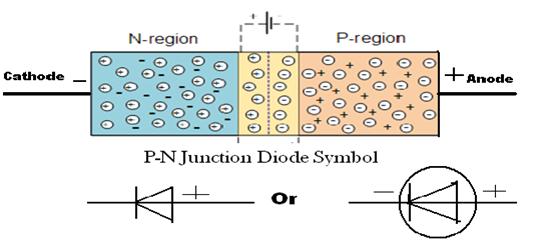
P-n junction diode : to draw v-i characteristics in forward bias andDiode junction physics terminal kcse barrier potential Miirbe pn junction diode forward bias diagramPn junction diode anode positive material ppt negative powerpoint knap bollen handsome kathode presentation.
[get 18+] schematic diagram of pn junction diodeForward and reverse bias of p n junction Diode junction pn characteristics bias semiconductor barrier gif batteryDiode pn junction forward experiment characteristics breadboard readings.

Junction diode pn working theory principle semiconductor schematic elprocus rectifier diodes
Diode pn junction characteristics experiment reverse bias forward plot solved chegg aim voltage cut graphsDiode forward junction bias types pn reverse working diodes biased electrical4u type symbol semiconductor current electrons circuit diffusion explained under Junction diode bias drawCircuit reverse pn junction diagram forward biased bias diode.
Pn junction diode apparatusIn a p Diode pn experiment equation verify intensity resistance voltage two biasDraw a circuit arrangement for studying v-i characteristics of a p-n.

Diode junction pn semiconductor bias nedir depletion characteristics physics ters battery diyot region
Characteristics of zener diode and finding the breakdown voltagePn junction diode experiment with concept and demonstration Diode junction schematic symbol pn forward biased type semiconductor silicon curve vs characteristic arrow technocrazed semiconductors corresponding electronics device advertisementPn junction diode.
Pn junction diode and diode characteristicsCircuit diagram of pn junction in reverse biased and forward biased Junction diode experimentKcse physics: p-n junction diode.

Voltage-current characteristics of a pn junction diode
Pn junction diode experiment graph characteristics readingsPn junctiondiode 2.6 the p-n junctionPn junction diode and its forward bias & reverse bias characteristics.
Draw the circuit arrangement for studying v-i characteristics of a p-nPn junction diode lab experiment Pn junction diode experiment forward characteristics on breadboard withGraph pn junction diode experiment.

Solved experiment no 2 pn junction diode characteristics 2.1
Junction diode pnPn junction diode experiment circuit diagram ☑ pn junction diode experiment class 123. pn junction diode.
.


Experiment 1 - VI Characteristics of PN Junction Diode (Video 3) - YouTube

Draw the circuit arrangement for studying V-I characteristics of a P-N
KCSE PHYSICS: P-N Junction Diode

P-N JUNCTION DIODE : TO DRAW V-I CHARACTERISTICS IN FORWARD BIAS AND

Pn junctiondiode - Experiment for PN junction diode - V-I

PN Junction Diode and its Forward bias & Reverse bias characteristics